
WNY STAMP

Schumer pitches top brass at Samsung on shovel-ready STAMP site for new semiconductor plant

By Press Release

Press release:

U.S. Senate Majority Leader Charles E. Schumer yesterday (Jan. 27) followed up on his efforts to secure a provision in the FY2021 National Defense Authorization Act to boost American-based semiconductor manufacturing by reaching out directly to Samsung, which is interested in possibly locating their new plant in Genesee County.

He called Senior Vice President of Samsung Device Solutions Joe Herr and other top brass about the Genesee Science and Technology Advanced Manufacturing Park -- STAMP -- in Alabama and expressed his strong support for the project coming to Western New York.

Samsung is currently considering the STAMP campus, as well as several other locations in other states, for its semiconductor fabrication (“fab”) plant – with 1,900 jobs – that the company plans to open late next year. Samsung’s Device Solutions division includes Samsung’s Global Semiconductor Foundry business. 

“This Samsung project is an exciting and a potential game changer for the region," Schumer said. "I made it clear to Samsung that I strongly support locating their planned 1,900 worker state-of-the-art semiconductor chip fab at the shovel-ready STAMP site in Genesee County. I know firsthand that STAMP is shovel-ready – and that, combined with Upstate New York’s robust semiconductor industry, make Genesee the perfect location for Samsung’s new chip fab.

World-class WNY Workforce

"Our world-class Western New York workforce combined with New York’s considerable experience in semiconductor manufacturing and R&D means STAMP is tailor-made to be the home for Samsung’s new facility. I stand ready to help Samsung harness all that the federal government has to offer to continue to lead the tech industry and position New York as a global hub of semiconductor manufacturing.

“When I stood at STAMP in August to announce my proposal to create the first-ever new federal semiconductor manufacturing and R&D incentives program, I said it could put sites like Western New York’s STAMP in contention for landing a new semiconductor manufacturing plant and the thousands of new jobs that come with it.

"This game-changer proposal passed into law last month and already companies like Samsung are considering STAMP for a 1,900 job chip fab plant, partly because of this new federal initiative. Now, I will work to secure this federal investment and offer my all-out support and advocacy in helping STAMP compete for this multi-billion-dollar plant.” 

Schumer has long championed the Genesee site and toured STAMP in August, and knows firsthand how ideal the campus would be as home for Samsung’s new chip fab. Schumer explained to Samsung that he, alongside the Genesee County Economic Development Center (GCECC), New York State, and Western New York officials, worked for a decade to help ensure that it was shovel-ready for a semiconductor facility.

WNY Offers: Low Utility Costs, Transportation Networks, Supplies Access, Brain Power

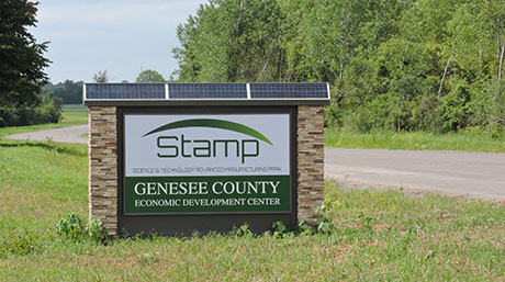
“The STAMP campus, sitting on 1,250 acres of land between Buffalo and Rochester, New York’s second and third largest metros, respectively, with a 1.2 million person world-class workforce, is specifically designed for large-scale fabs and provides maximum flexibility in layout and infrastructure connections,” Schumer said.

"Additionally, the senator pointed out many cost and infrastructure advantages to the STAMP campus location, including low utility costs, access to existing transportation networks, access to New York state’s existing chip fab supply chain ecosystem, and 62 colleges, universities, and community colleges within a two-hour drive of the site including Cornell University, University at Buffalo, Rochester Institute of Technology, University of Rochester, Genesee Community College.

Schumer said Samsung is relying on his legislation to building new fabs like this one in the United States. In fact, Schumer pointed out, the United States has gone from producing 24 percent of the world’s semiconductors in 2000, to just 12 percent while China, by comparison, has gone from producing zero chips to 16 percent of the world’s supply because the United States is not matching the investments that other competing nations are making in order to land new job-creating semiconductor chip fabs.

The senator's first-ever legislation will reverse this imbalance and level the playing field for companies like Samsung to build new chip fabs in the United States. For the first-time Schumer’s legislation will provide federal incentives to semiconductor chip fabs to build in the United States.

U.S. Reliance on Foreign-made Microelectronics Could Pose 'Huge Risks'

Upon passage of his legislation last month in the FY2021 National Defense Authorization Act Schumer said his legislation is vital. He noted that even though the United States revolutionized the microelectronic industry and invented nearly all of the key technology used to this day, by 2030, non-U.S. competitors are projected to control 83 percent of the global semiconductor manufacturing supply while domestic production could be less than 10 percent, threatening U.S. reliance on foreign-made microelectronics, which could pose huge risks to U.S. national and economic security.

In a recent meeting with the Commerce Secretary nominee, Governor Gina Raimondo, Schumer raised the urgent need to fully fund and implement the new Commerce semiconductor manufacturing grant program he passed into law as part of last year’s defense authorization, pointing to this Samsung investment as an example for why these federal incentives are such a high priority. Federal incentives are critical to the United States successfully competing with other countries, including China, for new semiconductor manufacturing investment like the proposed Samsung facility.

Schumer, in addition to paving the way for future federal incentives for investment into domestic semiconductor manufacturing previously brought STAMP to the attention of the Department of Defense, urging the agency to work with the semiconductor industry to expand the domestic supply of chips and other microelectronics.

STAMP is Made Specifically for What Samsung Needs

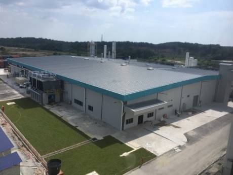
STAMP is specifically designed for development of large-scale semiconductor manufacturing. The 1,250 acre mega site can accommodate large advanced manufacturing operations with its expansive space for several plants.

Schumer has also previously lobbied the Board of Directors of the Semiconductor Industry Association (SIA) to put STAMP on their map and pitched SIA’s 18 semiconductor industry CEOs to look to expand their operations in Upstate New York at sites like STAMP in Genesee County.

In 2017 Schumer helped secure Federal Energy Regulatory Commission (FERC) approval of Empire Pipeline Inc.’s revised and extended PILOT agreement with Genesee County, the proceeds of which were needed to finance new water infrastructure at STAMP.

In 2016 Schumer began assisting STAMP secure necessary U.S. Fish and Wildlife right-of-way permits to construct new infrastructure hook-ups to STAMP. In 2012, Schumer successfully advocated on behalf of STAMP by calling on the U.S. Army Corps of Engineers to provide necessary wetlands permit assurances so that STAMP's developers could proceed with developing the site.

STAMP reportedly on Samsung's shortlist for $13 billion chip manufacturing plant

By Howard B. Owens

South Korean technology company Samsung is reportedly eyeing WNY STAMP, along with two locations in Texas, for the construction of a $13 billion chip manufacturing plant.

Citing The Wall Street Journal (paywall), The Hill reports, Samsung aims to become the leader in the $400 billion industry and needs a plant in the Uniited States to make that happen.

Sen. Charles Schumer was in Alabama in August to discuss a congressional push to increase semiconductor manufacturing in the United States as a matter of national defense. The National Defense Authorization Act has not yet been funded.

The Hill reports that Samsung is looking to negotiate with federal officials for financial incentives to build the plant in the United States because it would be cheaper to develop its product in other parts of the world. 

Reportedly, Samsung’s goal is to have a chip-making plant operational by October 2022 and to employ 1,900 people.

GCEDC staff outlines agency's progress for county legislators

By Howard B. Owens
Video Sponsor
.pane-node-body img {background: none !important; border: 0 !important; margin: 0 !important; padding: unset !important; padding-left: 1px !important } broadstreet.zone(69076)

The total annual tax revenue from all current Genesee County Economic Development Center-backed projects -- more than 160 since 2006 -- will generate more than $8.4 million in additional property tax revenue for local governments once all the projects have matured out of their PILOT phase.

There are more than 90 projects that received a PILOT (Payment In Lieu Of Taxes) that are now completely on the tax rolls.

A PILOT waives property taxes on the increase in assessed value associated with a building expansion or new construction but requires the property owner to make payments to the local taxing jurisdictions. 

The 71 projects currently with an active PILOT generated $1.5 million in revenue for local governments, such as municipalities, the county, and school districts, in 2019.

The projects with completed PILOTs generated another $3.5 million in revenue for local governments -- revenue that would not have been realized if the property owner had not expanded or started a new project causing an increase in the assessed value of the property.

Steve Hyde, CEO of GCEDC, Jim Krencik, marketing director, and Lezlie Farrell, CFO, shared data on GCEDC's progress during an annual review presentation for the county's Ways and Means Committee on Wednesday.

Hyde and Mark Masse, vice president of operations, both said Genesee County is well-positioned to take advantage of the new thinking among manufacturers in the post-pandemic world, when many companies realize they need to tighten up their supply chains and "reshore" (bring factories back to the United States) their operations. They're looking for shovel-ready sites, and there is ample such acreage in the GCEDC-created industrial parks around the county.

"Companies are taking a serious, hard look at where there are failings in the current system, from raw materials up through shipping," Masse said.

On a recent statewide conference call with three of the nation's top site selectors, one of them, whom Hyde described as the dean of site selectors, praised Genesee County.

"We've been working on getting on his radar for 10 years," Hyde said. "When you start to get on their radar, you've got a shot."

As for STAMP -- the industrial park in Alabama being marketed to tech manufacturers -- there are five companies currently considering siting a new facility there, including a semiconductor company that Hyde indicated Sen. Charles Schumer helped swing Genesee County's way.

These are long-term projects so Hyde said it will be a while before any of these potential suitors sign a deal.

The biggest obstacle to industrial growth in Genesee County is the lack of quality housing stock. That makes it harder to attract companies who want to ensure employees who move here can find quality housing or it means well-compensated employees move to Rochester or Buffalo.

Hyde noted that the average age of a house in Batavia is 73 years, twice the national average.

Construction work begins on final leg of water line to STAMP mega site

By Press Release

Press release:

Construction work has commenced to finish a major water line project to the Western New York Science & Technology Advanced Manufacturing Park (STAMP) and bring the STAMP South Campus to 100-percent shovel-readiness for development.

The Genesee County Economic Development Center (GCEDC) announced today (Aug. 18) that the $2 million active infrastructure project enables over one million gallons per day of water capacity to STAMP. This project is supported by Genesee County to support Phase I development of the STAMP site.

The 1,250-acre STAMP site, through the 850-acre STAMP North Campus and the 400-acre STAMP South Campus, is designed and permitted for more than six million square feet of new construction supported by low-cost hydropower.

“There is a tremendous amount of momentum for STAMP right now and not just from an infrastructure investment and construction standpoint, but in interest among site selectors and representatives from advanced manufacturing companies, including semiconductor companies from across the world,” said Steve Hyde, president and CEO, GCEDC. 

The start of the construction on the latest STAMP water line comes after U.S. Senator Charles Schumer was in Batavia on July 31st to announce among other things, his support for a $1 million grant through the Northern Border Regional Commission for the construction of a new force main to serve the entire STAMP site. 

STAMP infrastructure design, engineering and construction launched in 2014 with the allocation of $33 million by New York State.

“With federal, state and local funding enabling STAMP’s infrastructure delivery, our 1,250-acre mega site will provide a significant return on investment and can be a model for economic recovery as New York State emerges from the pandemic,” Hyde said.

The infrastructure work includes the completion of the construction of a water line that was started from a connection from the Erie County Water Authority in Pembroke near the New York State Thruway. The second leg included construction of the line at a connection near the Western New York National Cemetery for veterans, and now from the cemetery to the STAMP South Campus.  

The work is anticipated being completed by the end this year. The design and engineering work was performed by Clark Patterson & Lee.

For sake of national defense, Schumer pushes for semi-conductor plant at STAMP

By Howard B. Owens
Video Sponsor
.pane-node-body img {background: none !important; border: 0 !important; margin: 0 !important; padding: unset !important; padding-left: 1px !important } broadstreet.zone(69076)

In the video, Sen. Charles Schumer talks about the semiconductor plan, baseball, baseball trivia, his relationship with newly elected Rep. Chris Jacobs, the safety of reopening schools, and the future of the Muckdogs.

Press release:

Standing with local officials at Genesee’s STAMP* Campus, U.S. Senator Charles E. Schumer today unveiled his three-pronged push to jolt the U.S. semiconductor industry and the Upstate New York economy into high gear.

First, Schumer called for swift passage by Congress of the final Fiscal Year 2021 National Defense Authorization Act (NDAA), in which the senator successfully included an amendment that will continue U.S. leadership in semiconductor manufacturing and revitalize innovation in the global microelectronics sector.

Second, the Senator announced his push for a $1M Northern Border Regional Commission grant that STAMP needs to construct a new sewer line to complete STAMP’s wastewater system infrastructure. The sewer is the final piece of infrastructure that will make the 1,250-acre STAMP campus shovel-ready for manufacturing facility construction.

Third, Schumer will urge the Department of Defense (DoD) to consider the STAMP campus as the agency looks to partner with industry to develop new domestic semiconductor fabs. Combined, the Senator’s efforts will provide unprecedented support for the U.S. semiconductor industry and create opportunities to bring hundreds of jobs to Genesee County and Upstate New York.

“The economic and national security risks posed by relying too heavily on foreign semiconductor suppliers cannot be ignored, and Upstate New York, especially the STAMP Campus here in Genesee, is the perfect place to grow this industry by leaps and bounds,” Senator Schumer said.

“We must continue to invest in our domestic semiconductor industry in order to keep good-paying, high-tech American manufacturing jobs here in Upstate New York. We need to ensure our domestic microelectronics industry can safely and securely supply our military, intelligence agencies, and other government needs. This is essential to American jobs, our national security, and to U.S. leadership in this critical industry."

Schumer noted that even though the United States revolutionized the microelectronic industry and invented nearly all of the key technology used to this day, competitors in Asia, especially China, have made huge investments into their microelectronics industries in recent years to challenge and undercut U.S. leadership.

In fact, Schumer pointed out, the United States has gone from producing 24 percent of the world’s semiconductors in 2000, to just 12 percent more recently. In contrast, China has gone from producing zero chips to 16 percent of the world’s supply in the same time frame. The senator warned that by 2030, Asia is projected to control 83 percent of the global semiconductor manufacturing supply while domestic production could be less than 10 percent, threatening U.S. reliance on foreign-made microelectronics, which could pose huge risks to U.S. national and economic security.

Therefore, Schumer argued, his three-pronged plan to revitalize the semiconductor industry and incentivize it to build new research and manufacturing facilities in the United States at sites like STAMP is vital to cement global U.S. leadership in the microelectronics industry and will ease U.S. reliance on foreign-made semiconductors, alleviating economic and national security risks.

“Senator Schumer’s leadership in the Senate’s passage of the American Foundries Act as a part of the National Defense Administrative Act will help put STAMP over the finish line as it will make available necessary funding to develop and construct the final pieces of infrastructure to stand up multiple semiconductor manufacturing fabs and along with it the creation of thousands of good-paying, family-sustaining jobs to Genesee County and the Western New York and Finger Lakes regions,” said GCEDC President and CEO Steve Hyde. Attracting semiconductor and similar industries at STAMP will result in as much as $10 billion to $15 billion of private sector investment all of which will be enabled by this game-changing legislation.”

Secondly today, Schumer announced his push to secure the Northern Border Regional Commission (NBRC) grant to construct the last missing sewer line needed for STAMP to achieve shovel-ready status. Specifically, this funding is needed to complete STAMP’s sewer and wastewater system by constructing a 14,500-square-foot force main sewer line to support new businesses that locate at STAMP. The force main is the final piece needed to make STAMP shovel-ready with the capabilities to meet any industry’s needs to construct new manufacturing operations at STAMP and create new high-quality jobs. 

Lastly, Schumer called on the Department of Defense (DoD) to consider STAMP as a location for next-generation semiconductor research and manufacturing facilities now that the DoD is in discussions with semiconductor manufactures to build new domestic chip manufacturing facilities to ensure U.S. leadership in the global microelectronics supply chain.

Last month Schumer wrote to Defense Secretary Mark Esper to draw his attention to the opportunities for new Semiconductor development at STAMP. As a result, DoD officials participated in a meeting Schumer convened with STAMP officials to help position STAMP to capitalize on new opportunities through the DoD to attract semiconductor research and manufacturing facilities to STAMP.

Following Schumer’s unveiling of his bipartisan American Foundries Act and major push to bolster U.S. leadership in the microelectronics sector, he successfully advanced his proposal as an amendment included in the Senate-passed Fiscal Year 2021 National Defense Authorization Act (NDAA). The amendment:

  • Directs the Secretary of Commerce to create a grant program for constructing, expanding, or modernizing commercial semiconductor fabrication, assembly, testing, packaging, and advanced R&D facilities in the United States.
  • Directs the Secretary of Defense to create a partnership program with the private sector to encourage the development of advanced, measurably secure microelectronics for use by the Department of Defense, Intelligence Community, critical infrastructure, and other national-security applications.
  • Requires the Secretary of Commerce to commence a review within 120 days assessing the state of the U.S. semiconductor industrial base.
  • Establishes a Multilateral Microelectronics Security Fund, with which the United States, its allies, and partners will work to reach agreements promoting consistency in their policies related to microelectronics, greater transparency including supply chains, and greater alignment in export control and foreign direct investment policies.
  • Directs the President to establish a subcommittee on semiconductor technology and innovation within the National Science and Technology Council; directs the Secretary of Commerce to establish a national semiconductor technology center to conduct research, fund semiconductor startups and a Manufacturing USA Institute, create a National Advance Packaging Manufacturing Program; and encourages the Secretary of Labor to work with the private sector on workforce training and apprenticeships in semiconductor manufacturing.

This amendment, which is also cosponsored by U.S. Senator Kirsten Gillibrand, is based on the Senator’s bipartisan American Foundries Act, which has been broadly supported by key players in New York’s semiconductor industry, including GlobalFoundries, IBM, ON Semiconductor, Cree Inc., the Genesee County Economic Development Center, Hudson Valley Economic Development Corporation, Mohawk Valley EDGE, Cornell University, Binghamton University, and SUNY Polytechnic Institute.

 STAMP is specifically designed for development of large-scale semiconductor manufacturing. The 1250-acre mega site is divided into an 850-acre North Campus that can accommodate clean tech advanced manufacturers including up to three semiconductor chip fabs and a 400-acre South Campus ideal to attract new food, beverage, and warehouse/distribution development.

In 2012, Schumer successfully advocated on behalf of STAMP by calling on the U.S. Army Corps of Engineers to provide necessary wetlands permit assurances so that STAMP's developers could proceed with developing the site. In 2017 Schumer helped secure Federal Energy Regulatory Commission (FERC) approval of Empire Pipeline Inc.’s revised and extended PILOT agreement with Genesee County, the proceeds of which were needed to finance new water infrastructure at STAMP.

*STAMP -- Science and Technology Advanced Manufacturing Park

Schumer, Gillibrand: Defense bill will jolt U.S. semiconductor industry and Genesee County region’s economy into high gear

By Billie Owens

Press release:

Following Senator Charles E. Schumer’s unveiling of his bipartisan American Foundries Act and major push to bolster U.S. leadership in the microelectronics sector, Schumer and U.S. Senator Kirsten Gillibrand today announced the Fiscal Year 2021 National Defense Authorization Act (NDAA) includes their provision to reestablish U.S. leadership and revitalize innovation in the global microelectronics sector.

The senators explained that the bipartisan legislation increase federal investment into semiconductor manufacturing by providing new federal incentives to conduct advanced research and development of semiconductor technology, secure the supply chain, and ensure national and economic security by reducing reliance on foreign semiconductor manufacturing.

The amendment passed in the Senate 96-4 yesterday, and the legislation included in the final NDAA, which is expected to be put to a final vote in the Senate in coming days, will provide unprecedented support for the U.S. semiconductor industry.

“The economic and national security risks posed by relying too heavily on foreign semiconductor suppliers cannot be ignored, and Upstate New York, which has a robust semiconductor sector, is the perfect place to grow this industry by leaps and bounds,” Senator Schumer said.

“America must continue to invest in our domestic semiconductor industry in order to keep good-paying, high-tech American manufacturing jobs here in Upstate New York. We need to ensure our domestic microelectronics industry can safely and securely supply our military, intelligence agencies, and other government needs.

"This is essential to our national security and to U.S. leadership in this critical industry. I’m pleased to deliver this win in this year’s final NDAA for Upstate New York and the entire country."

“Our nation is in an economic crisis. Investing in microelectronics manufacturing and the semiconductor industry will create high paying manufacturing jobs for hard working Americans at a time when our country needs it most,” Senator Gillibrand said.

“This amendment will help expand our advanced manufacturing workforce in Upstate New York and invest in cutting edge research and development. I’m proud that this legislation is included in NDAA so that we can continue to strengthen our microelectronic domestic supply chain, prioritize American-owned businesses over foreign production, and keep our country safe.”  

The senators noted that even though the United States revolutionized the microelectronic industry and invented nearly all of the key technology used to this day, competitors in Asia, especially China, have made huge investments into their microelectronics industries in recent years to challenge and undercut U.S. leadership.

In fact, Schumer and Gillibrand pointed out, the United States has gone from producing 24 percent of the world’s semiconductors in 2000, to just 12 percent more recently. In contrast, China has gone from producing zero chips to 16 percent of the world’s supply in the same time frame.

The senators warned that by 2030, Asia is projected to control 83 percent of the global semiconductor manufacturing supply while domestic production could be less than 10 percent, threatening U.S. reliance on foreign-made microelectronics, which could pose huge risks to U.S. national and economic security.

Schumer has long-championed increased efforts to expand the domestic microelectronics industry, supporting companies like GlobalFoundries, which houses their most advanced "Fab 8" manufacturing facility in Malta, New York, IBM, and others.

With New York home to multiple major companies and research institutions in the semiconductor industry, the state is positioned to securely supply the U.S. government with critical technologies and maintain U.S. leadership in this technology. This is a tremendous opportunity for New York’s semiconductor companies to expand operations, create more jobs in Upstate New York, and help the U.S. reduce its reliance on foreign semiconductor manufacturing.

Specifically, supporters of the amendment include: GlobalFoundries; IBM; ON Semiconductor; Cree Inc.; the Genesee County Economic Development Center; Hudson Valley Economic Development Corporation; Mohawk Valley EDGE; Cornell University; Binghamton University; and SUNY Polytechnic Institute.

“Senator Schumer has been a longtime champion of New York's 1,250-acre STAMP megasite in Genesee County and this legislation provides a tremendous opportunity to create thousands of high-quality semiconductor jobs for the Western New York and Finger Lakes regions," said Steve Hyde, president and CEO of the Genesee County Economic Development Center (GCEDC). "In short, STAMP* is a transformative economic development game-changer that will generate billions of dollars of economic activity across Upstate New York.

"We appreciate Senators Schumer and Gillibrand’s push to pass this milestone legislation that advances our site, region, and New York's readiness as we compete globally for projects of this scale.” 

*STAMP: Western New York Science and Technology Advanced Manufacturing Park in Alabama.

Details on the NDAA Amendment are below:

  • Directs the Secretary of Commerce to create a grant program for constructing, expanding, or modernizing commercial semiconductor fabrication, assembly, testing, packaging, and advanced R&D facilities in the United States.
  • Directs the Secretary of Defense to create a partnership program with the private sector to encourage the development of advanced, measurably secure microelectronics for use by the Department of Defense, Intelligence Community, critical infrastructure, and other national-security applications.
  • Requires the Secretary of Commerce to commence a review within 120 days assessing the state of the U.S. semiconductor industrial base.
  • Establishes a Multilateral Microelectronics Security Fund, with which the United States, its allies and partners will work to reach agreements promoting consistency in their policies related to microelectronics, greater transparency including supply chains, and greater alignment in export control and foreign direct investment policies.
  • Directs the president to establish a subcommittee on semiconductor technology and innovation within the National Science and Technology Council, directs the Secretary of Commerce to establish a national semiconductor technology center to conduct research, fund semiconductor startups and a Manufacturing USA Institute, create a National Advance Packaging Manufacturing Program, and encourage the Secretary of Labor to work with the private sector on workforce training and apprenticeships in semiconductor manufacturing.

Schumer warns of relying on foreign-made semiconductors, calls for building robust, resilient microelectronics industry

By Billie Owens

Press release:

Citing concerns that China is catching up to the United States in microelectronics production capacity, U.S. Senator Charles E. Schumer today (June 28) unveiled the American Foundries Act, a bipartisan initiative that seeks to reestablish U.S. leadership and revitalize innovation in the global microelectronics sector.

Schumer explained that the bipartisan legislation would make critical investments in domestic commercial and defense-related microelectronics manufacturing and research and development, and address economic and national security concerns by decreasing U.S. dependence on foreign-made semiconductor chips.

“The economic and national security risks posed by relying too heavily on foreign semiconductor suppliers cannot be ignored, and Upstate New York, which has a robust semiconductor sector, is the perfect place to grow this industry by leaps and bounds,” Senator Schumer said. “America must continue to invest in our domestic semiconductor industry, including companies like GlobalFoundries, ON Semiconductor, IBM and Cree right here in New York, in order to keep good-paying, high-tech American manufacturing jobs here at home.

"We need to ensure our domestic microelectronics industry can safely and securely supply our military, intelligence agencies, and other government needs. This is essential to our national security and to U.S. leadership in this critical industry."

The senator noted that even though the United States revolutionized the microelectronic industry and invented much of the key technology used to this day, competitors in Asia, especially China, have made huge investments into their microelectronics industries in recent years to challenge U.S. leadership. In fact, Schumer pointed out, 78 percent of cutting-edge wafer fabrication capacity is now based in Asia, with last year being the first year that North America fell behind China.

Schumer has long-championed increased efforts to expand the domestic microelectronics industry, supporting companies like GlobalFoundries, which houses their most advanced "Fab 8" manufacturing facility in Malta, New York, IBM, and others.

With New York home to multiple major companies and research institutions in the semiconductor industry, the state is positioned to securely supply the U.S. government with critical technologies and maintain U.S. leadership in this technology, offering a tremendous opportunity for New York’s semiconductor companies to expand operations, create more jobs in Upstate New York, and help the United States reduce its reliance on foreign semiconductor manufacturing.

Specifically, supporters of the American Frontiers Act include GlobalFoundries, IBM, ON Semiconductor, Cree Inc., the Genesee County Economic Development Center, Hudson Valley Economic Development Corporation, Mohawk Valley EDGE, Cornell University, Binghamton University, and SUNY Polytechnic Institute.

"We applaud the powerful American Foundries Act of 2020 co-sponsored by Senator Schumer and the impressive, bipartisan list of Senate leaders,” said Tom Caulfield, CEO of GlobalFoundries. “Senator Schumer has supported semiconductor manufacturing and GlobalFoundries for many years and this legislation seeks the quickest route to boosting chip production in the U.S. We appreciate this timely and significant contribution as Congress and the Administration work through the best approach for federal investment to restore domestic leadership in semiconductor manufacturing.”

"The U.S. semiconductor industry drives economic growth through technological breakthroughs and plays a critical role in the nation’s security,” said John E. Kelly III, Executive Vice President, IBM. “IBM strongly supports the American Foundries Act of 2020 because this important legislation would sustain American leadership in semiconductor technology and establish a national strategy to move it forward. We thank Senators Schumer and Cotton for their leadership on this bill and urge the Senate to pass it quickly."

“The American Foundries Act is a bold step to respond to the aggressive incentives available to overseas competitors and reverse the decline of semiconductor manufacturing in the United States,” said Keith Jackson, president and CEO of ON Semiconductor. “ON Semiconductor urges the Congress to quickly advance legislation to promote American semiconductor research and manufacturing.”

“Cree continues to invest aggressively in silicon carbide manufacturing and research in order to support the growing, global demand for our technologies, and we believe advanced semiconductor manufacturing is essential to leading the acceleration of critical next-generation technologies," said Gregg Lowe, president and CEO of Cree Inc. "Like many other semiconductor companies in the U.S., we believe this legislation would provide necessary investments that move our industry and economy forward and we commend its introduction."

"Senator Schumer has long recognized that our 1250-acre STAMP site in Genesee County presents a tremendous opportunity to create thousands of high quality semiconductor jobs for the Western New York and Finger Lakes regions," said Steve Hyde, president and CEO of the Genesee County Economic Development Center (GCEDC).

"Our challenge has always been the considerable cost to get the site developed and shovel ready in the global competition to land projects of this scale. This legislation though is a game changer in so many ways as it will support cutting-edge domestic semiconductor development and increases in semiconductor manufacturing capacity at a crucial time in our nation's history."

“Senator Schumer’s American Foundries Act is the type of innovative, bipartisan legislation that we need to build on our regional strengths and grow the Hudson Valley economy post-pandemic," said Mike Oates, president and CEO of Hudson Valley Economic Development Corporation. "With industry leaders like IBM, GlobalFoundaries, and soon ON Semiconductor right here in the Hudson Valley, it is no secret that investing in the microelectronics manufacturing and research and development space will enhance our ability to manufacture semiconductor chips, create jobs, and reimage our economy.

"HVEDC is proud to support Senator Schumer in his push to bolster our footprint in the growing semiconductor sector and we will continue working with him to keep the Hudson Valley on the map as a global industry leader.”

“Construction of new microelectronics and semiconductor fabrication facilities have the ability to change the economic landscape of a region and the proposed American Foundries Act proposed by Senator Schumer is a strategic investment to secure the United States’ position as a global  leader in microelectronics and semiconductor R&D,” said Steven J. DiMeo, president, Mohawk Valley EDGE.

“As our economy shifts away from the long-standing model of industrialism coupled with the uncertainty of a global pandemic, we now more than ever need the federal government to continue its support of game-changing industries like semiconductors and microelectronics. The construction of Cree’s state-of-the-art 200 mm enabled SiC semiconductor facility at the Marcy Nanocenter in Upstate NY, is a pivotal example of what can be done when all stakeholders are working together to advance our high-tech ecosystem and regional economy and maintain the United States’ global competitiveness.”

Emmanuel P. Gianellis, vice provost for Research and Vice President for Technology Transfer, Intellectual Property and Research Policy at Cornell University, said, “Senator Schumer has long recognized that the best way to keep America at the forefront of the technology revolution is to invest in research and development here at home.

"Not only does the American Foundries Act of 2020 direct critical resources into expanding the domestic production of microelectronics, it also points the way to the future with substantial funding for research and innovation. Cornell University is pleased to support this legislation and commends Senator Schumer for his leadership.”

"Whether we are talking about technology that enables advancement in AI for autonomous vehicles, smart energy for a greener environment or flexible wearable devices for human health and industrial monitoring, the United States government must remain on the frontlines, supporting industrial and academic innovations in advanced electronics manufacturing," said Harvey Stenger, president of Binghamton University.

"We once again acknowledge all that Sen. Schumer has done and continues to do to emphasize the importance of research and development efforts in private labs as well as at research institutions like Binghamton University. We thank the senator for this latest effort to apply resources to enhance the bridge from early R&D to at-scale manufacturing that will lead to breakthroughs in next-generation semi-conductor research and keep the United States competitive and a leader in the global economy."

“Leadership in the microelectronics industry is critical for America’s continued economic and strategic competitiveness on the global stage," said SUNY Polytechnic Institute Interim President Grace Wang, Ph.D. "The American Foundries Act of 2020 will provide a more strategic national approach in advancing  microelectronics capabilities, R&D, and workforce development and ensure our nation remains at the forefront of impactful innovation.

"This bill takes a bold approach to facilitate chip fab modernization efforts and investment in key areas such as fabrication, assembly, test, and advanced packaging to strengthen our nation’s technological independence and agility for years to come.”

Schumer said he will aim to include the legislation as an amendment in this year’s National Defense Authorization Act (NDAA).

Senator Schumer introduced the American Foundries Act of 2020 in the Senate, along with Senators Cotton (R-Arkansas), Reed (D-Rhode Island), Hawley (R-Missouri), Gillibrand (D-New York), Risch (R-Idaho), Jones (D-Alabama), Collins (R-Maine), King (I-Maine), and Rubio (R-Florida), and details of the bill can be found below:

Support for Commercial Microelectronics Projects: Authorizes the Department of Commerce to award $15 billion in grants to states to assist in the construction, expansion, or modernization of microelectronics fabrication, assembly, test, advanced packaging, or advanced research and development facilities.

Support for Secure Microelectronics Projects: Authorizes the Department of Defense to award $5 billion in grants for the creation, expansion, or modernization of one or more commercially competitive and sustainable microelectronics manufacturing or advanced research and development facilities capable of producing measurably secure and specialized microelectronic for defense and intelligence purposes. This funding may go to primarily commercial facilities capable of producing secure microelectronics.

R&D Funding: Authorizes $5 billion in R&D spending to secure U.S. leadership in microelectronics. Requires agencies that receive this funding to develop policies to require domestic production, to the extent possible, for any intellectual property resulting from microelectronics research and development as a result of these funds.

The new R&D funding would be broken up as follows:

  • $2 billion for DARPA’s Electronics Resurgence Initiative
  • $1.5 billion for the National Science Foundation
  • $1.25 billion for the Department of Energy
  • $250 million for the National Institute of Standards and Technology

National Microelectronics Research Plan: Establishes a subcommittee of the President’s Council on Science and Technology to produce a report each year to guide and coordinate funding for breakthroughs in next-generation microelectronics research and technology, strengthen the domestic microelectronics workforce, and encourage collaboration between government, industry, and academia.

Safeguards: Prohibits firms owned, controlled or otherwise influence by the Chinese government from accessing funds provided by the legislation.

'It's a new world': County planners put stamp of approval on mixed-use buildings in Town of Pembroke district

By Mike Pettinella

The Genesee County Planning Board on Thursday night recommended approval of a zoning text amendment to allow mixed-use buildings in the Town of Pembroke Interchange District, but not before a discussion on the practice of placing housing units in industrial parks.

Tom Schubmehl, a member of the planning board and Pembroke resident, said he had some reservations about the Town Board’s application to modify zoning in the Interchange District -- a wide area around Thruway Exit 48A, extending to Route 5 along Route 77.

“Is there any other district in the county industrial districts that allows residential use? Schubmehl asked, directing his question to County Planning Director Felipe Oltramari.

Oltramari said that the Interchange District was different from a traditional industrial district.

“It can have commercial and it can have industrial … it has the Flying J (Travel Center). It has other things like that and includes an industrial park from the EDC,” Oltramari said, adding that he couldn’t think of other similar areas in the county that permit mixed-use facilities.

Schubmehl said he couldn’t either and said “it is a concern of mine that we start letting residential fill in this space. It's going to be no different than the rest of Pembroke.”

“I know it has no bearing on the impact of inter-community that we're discussing here tonight as a County Planning Board, but as a resident of Pembroke, I think it's bad idea,” he stated.

$3 Million Commercial/Resident Project Proposed

The Genesee County Economic Development Center is touting a $3 million commercial/residential project at its Buffalo East Technology Park, which is situated in the Interchange District.

J & R Fancher Property Holdings LLC has proposed building a 32,254-square-foot, three-story facility on two acres in the park, and is waiting for a public hearing and GCEDC board vote on its application to receive more than $600,000 in property, sales and mortgage tax incentives.

According to the GCEDC, the project consists of 17 market-rate, one- and two-bedroom apartments on the second and third floors, with space for four commercial tenants, as well as indoor parking and a fitness center on the ground floor.

Chris Suozzi, GCEDC vice president of business development, was on the planning board’s Zoom videoconference meeting last night, and pointed out that his agency worked with the Town of Pembroke on attracting the venture.

“They were all in favor for it,” Suozzi said. “Certainly, there's a housing shortage need in Genesee County. If anybody hasn't seen the housing study that LaBella (Associates) put out, (it’s) on the Genesee County website. And there's a big shortage of housing.”

GCEDC: 'Live, Work, Play' Model

Suozzi said the GCEDC is promoting a “live, work, play model” and that housing – particularly at industrial parks -- is an essential component in that thinking.

“And I know the location … in Pembroke is a great location because it's across from the school and already has a Tim Hortons that wasn't part of the EDC project, but it has that ability to be right next door to it and also has 7.9 acres in total that is being proposed, of which 2 (acres) are buildable and the other 5.9 are wetlands,” Suozzi offered. “They're all protected. It's a green space.”

He went on to say the project will generate tax revenue for the Town of Pembroke and reiterated that the town board is endorsing it.

Schubmehl then asked Suozzi if the GCEDC was going to consider residential at the WNY Science & Technology Advanced Manufacturing Park (STAMP) in the Town of Alabama.

“Well, you know, if the town said yes, I would certainly look at it, but it's not really up to Chris Suozzi and it’s not up to the EDC -- it's up to the municipality,” he said, again referencing a housing shortage.

“We look at economic development as a whole, and we bring in these companies … and the workers are living in Rochester and Buffalo, (so) we’re not optimizing the economic benefit of Genesee County,” he said. “And that's what that housing studies are showing; (that) there's a big need and we're missing the boat in terms of that revenue staying right in our county.

“So, to me, this is a new world right now and housing’s a big part of it, and the 'live, work, play' model is starting to change what's going on Downtown Buffalo right now … It's because all these old factories are being recondition and rehabbed and the millennials are jumping all over them and they're seeing growth in their workforce.”

Director Promotes Mixed Use for STAMP Site

Oltramari said he could foresee mixed-use buildings at the STAMP site, especially in a technology district closest to the hamlet of Alabama.

“I could see mixed-use buildings in that because the whole point of that is sort of having like an actual link between the hamlet and the business park,” he said. “You could have commercial businesses on the bottom floor, sort of like a main street kind of scenario. And I think that's been the vision for, you know, that kind of part of the park for a while now. So, I think even the town would be in favor of that at STAMP.”

Schubmehl asked whether or not the “live, work” model was actually in the proposal in front of the board, which prompted Oltramari to say he didn’t see it as a major issue.

“I think the era of separating uses, just for the sake of it commercial from residential or, you know, the whole reasoning behind that is to keep incompatible uses apart,” he said. “I don’t see that as a reason anymore, especially in the business parks.”

Planning Board Chair Laraine Caton then asked for a vote and all members, including Schubmehl, voted in favor of the request.

“No, I'm not opposed to it for the purposes as a planning board, we’re worried about inter-community problems here,” Schubmehl said. “And that's not an inter-community problem.”

In other action, planners:

-- Recommended approval with modifications of a special use permit for Jesse and Jolene Coots of Le Roy to operate an ATV, automotive event, hill climb, mud bog and time trial course on 10 acres of a 110-acre vacant parcel of land that they own on Perry Road in Pavilion.

The applicants said they plan to hold events two or three times this year (with the schedule dependent upon the COVID-19 pandemic).

The board’s modifications focus on the applicant obtaining written documentation from NYS Department of Conservation that the project will not be encroaching on wetlands as well as a permit from the Army Corps of Engineers for the potential Federal Wetlands. It also asks that the Coots submit an application for 9-1-1 Address Verification to the Genesee County Sheriff's Office to ensure that an address is assigned that meets Enhanced 9-1-1 standards.

-- Recommended approval with modifications of a special use permit request from Waifin Properties LLC of Clarence Center to operate a contractor’s yard in a Commercial District at 850 Main Road, Pembroke.

The proposed yard would encompass a 100-foot by 100-foot area on a 7.6-acre lot.

The board said the applicant is required to surround equipment and materials storage area with a fence of at least 8 feet high that has a gate, which shall be closed and locked except during working hours.

WNY STAMP touted at Semicon Europa in Munich, Germany

By Billie Owens

Press release:

The Genesee County Economic Development Center (GCEDC) recently participated in Semicon Europa, the largest European semiconductor industry event connecting leaders across the advanced manufacturing world and related supply chains. 

Director of Marketing and Communications Jim Krencik represented the GCEDC and the Western New York Science & Technology Advanced Manufacturing Park (WNY STAMP) at the event, which was held in Munich, Germany Nov. 12th through Nov. 15th.

More than 8,000 industry professionals participated in the conference. Krencik participated in the event as part of the New York Love Nanotech pavilion, which included representatives from Empire State Development’s Strategic Business Division, SUNY POLY/NY CREATES, AIM Photonics, site developers, and New York-based supply chain companies, with the support of National Grid.

While connecting with representatives of semiconductor industry companies from North America, Europe, and Asia, Krencik was able to tout many of WNY STAMP’s assets, such as low-cost hydropower, site infrastructure development, and the availability of top-end talent in the region.

“New York State has proven to be an ideal location for the industries represented at Semicon Europa,” Krencik said. “The assets available at Western New York Science & Technology Advanced Manufacturing Park provide a ready source for the growth of the semiconductor industry and advanced manufacturing in our region.”

Located in Alabama, Genesee County, WNY STAMP is a 1,250-acre campus connecting New York’s second- and third-largest metropolitan areas, and developed to best serve the needs of advanced manufacturing projects. Ongoing site development will enable WNY STAMP to achieve full capabilities of 485-megawatts electric capacity and 11-million gallons per day of water capacity.

Heading east: Wendt's Propane & Oil a step closer to expansion in Le Roy

By Mike Pettinella

The Genesee County Planning Board tonight voted in favor of a special use permit for a family-owned propane business that is branching out to the Town of Le Roy.

The board unanimously approved the permit for Wendt’s Propane & Oil to install an above-ground propane distribution center at OATKA Hills 1 Commerce Park on North and Lake Roads in Le Roy, agreeing that the project should pose no significant county-wide or inter-community impact.

It was recommended, however, that Town of Le Roy officials alert the fire district of the plan and that the applicant submit documentation pertaining to 9-1-1 address verification requirements and to meet Enhanced 9-1-1 standards.

Company President Paul Wendt and his son, Trevor, sales manager, attended the meeting along with David Ciurzynski, of Ciurzynski Consulting LLC, in Attica.

“Our office is in Sanborn but we have been delivering more and more this way,” said Paul Wendt, noting that the Le Roy facility will be their first venture away from Niagara County. “We found a nice piece of property in Genesee County and we thought that it would be good to expand.”

Wendt said three employees initially will work at the Le Roy site, which (mirroring its home base) will provide propane and oil service for commercial, residential and agricultural customers.

According to documents filed with the planning board, the plan is to develop around six acres of the parcel for the above-ground storage tanks and 9,600-square-foot warehouse and truck garage building. The rest of the 11.9-acre tract will remain undeveloped, with an eye on creating walking paths and green space.

Ciurzynski said they hope to have the tanks installed in November and have the building up by next spring. First, they have to get the Town of Le Roy's approval of the special use permit and then apply for the necessary building permits.

The Wendts’ project is set up in two phases – the first to get the site ready for the installation of a pair of 30,000-gallon storage tanks, with four additional locations for future expansion, and the second to put up the warehouse and truck garage.

In other action, planners recommended:

-- Approval of a special sign permit for a third sign at Metro Mattress at 4187 Veterans Memorial Drive in the Town of Batavia. While the maximum number of signs normally is two, the board felt the extra sign would not cause any problems.

Documentation submitted by Craig Tesler of Premier Sign Systems showed three freestanding lighted signs would be affixed to the building – at dimensions of approximately 4 x 10 feet, 3 ½ by 24 feet, and 3 ½ by 7 ½ feet.

-- Approval of an ice cream stand to be operated by Amanda Smith, of Darien, on property owned by John Mroz at 9114 Alleghany Road (Route 77) in the Town of Pembroke.

-- Approval of a site plan review for relocation of a doctor’s office to a building owned by Nancy Crocker at 7133 W. Main Road (Route 5) in the Town of Le Roy. The 4,460-square-foot structure sits on 3.1 acres and meets medical code requirements, the owner said.

-- Approval of the final subdivision to transfer a roadway at the WNY Science &Technology Advanced Manufacturing Park from routes 77 and 63 to Crosby Road (STAMP Drive) in the Town of Alabama from the Genesee County Economic Development Center to the Genesee County Highway Department.

GCEDC approves nearly $30 million budget, bulk of it for STAMP infrastructure

By Billie Owens

Press release:

The Board of Directors of the Genesee County Economic Development Center (GCEDC) adopted their 2020 budget at a board meeting today, projecting expenditures of $29.7 million.

The budget includes $25.5 million in grants for the development of infrastructure at the Western New York Science and Technology Advanced Manufacturing Park (WNY STAMP).

Of that total, $20.2 million is dedicated to the advancement of Phase I infrastructure at the campus (remaining funds from the original $33 million state allocation); and $5.3 million is dedicated to the advancement of Phase II infrastructure (initial funds from the $8 million Empire State Development grant).

The 1,250-acre WNY STAMP campus in the Town of Alabama is the largest high-tech greenfield site in New York, and connects low-cost hydropower, large-scale infrastructure, and the Buffalo-Rochester Metro Corridor’s workforce talent.

“The GCEDC is building WNY STAMP to be a market-ready site, and a catalyst for the success of the people of Genesee County and companies that will create a stronger future for our region,” said Paul Battaglia, chairman of the GCEDC.

As a public benefit corporation, the GCEDC generates fees from economic development projects and other sources to run the agency’s operations, programs and services.

The GCEDC anticipates $375,000 in revenues from project origination fees and $3,800 in revenues from revolving loan fund interest; $300,000 in annuities from projects approved in previous years.

Revenues also include $300,000 that will be received from the Genesee Gateway Local Development Corporation (GGLDC), and $50,000 anticipated from the Genesee County Funding Corporation, to support the agency’s overall Economic Development Program.

“There is a large body of work that occurs at this agency each year, and I am pleased that we continue to find resourceful ways to serve the businesses and citizens of Genesee County,” said Lezlie Farrell, CFO of the GCEDC.

“Operating expenditures have been controlled and reduced wherever possible.”

The GCEDC budget anticipates a $233,000 allocation by Genesee County to support economic development and a growing return on investments to the county.

In 2018, the last full year of data available, GCEDC projects (current and expired) produced more than $4.4 million in combined PILOT -- Payment In Lieu Of Taxes -- payments and property taxes to local taxing jurisdictions.

“Genesee County is a vital partner in our efforts to bring new business and growth to our region," Battaglia said. "We rely on the Genesee County Legislature to support our budget and operations so we can continue to enable business and community success.

"In 2018, Genesee County benefited from $19 returned on every one dollar allocated to GCEDC operations.”

GCEDC takes part in cutting-edge Semicon West conference in San Francisco

By Billie Owens

Submitted photo and press release:

Officials from the Genesee County Economic Development Center (GCEDC) once again made the annual trip to the New York Loves Nanotech Summit at Semicon West at the Moscone Center in San Francisco July 8-11.

GCEDC Vice President of Business and Workforce Development Chris Suozzi participated in a panel discussion with other economic development professionals about how infrastructure investments are advancing New York’s impact on the development and commercialization of emerging and existing technologies.

Suozzi highlighted investments at the Western New York Science and Technology Advanced Manufacturing Park (WNYSTAMP), the 1,250-acre high-tech greenfield developed in Alabama.

“Semicon West is a great event for us to not only talk about all the great economic development initiatives occurring in Genesee County, but across New York State,” Suozzi said. “New York is continuing to make investments in semiconductor infrastructure and the Buffalo-Rochester Metro Corridor stands out as an area that is providing the best workforce and STEM education in the country.”

New York State is at the forefront of advancing AI, quantum computing, power electronics, and neuromorphic computing capabilities through their advancements in process, equipment, materials and device technology-related research. 

Suozzi and GCEDC Director of Marketing and Communications Jim Krencik also led discussions with representatives of semiconductor and advanced manufacturing businesses seeking to invest in Genesee County and the talent-rich Buffalo-Rochester Metro Corridor.

Suozzi and Krencik were joined at Semicon West by New York Loves Nanotech, a statewide group led by economic development organizations, academic institutions, and technology companies. NYLN promotes WNY STAMP and the state’s assets to high-tech companies.

“Through our presence at this annual event and the relationships with have established with officials from advanced manufacturing companies, Genesee County’s assets will be well received as these officials are discussing ideal locations for their operations,” Krencik said.

For the 22nd year, NY Loves Nanotech had a large delegation of more than 60 officials attending the industry conference. NY Loves Nanotech, Empire State Development (ESD) and National Grid hosted a pavilion at the industry leading conference, which they co-exhibited with several other companies and organizations.

So far, New York has attracted more than $20 billion in nano-optics, photonics, and semiconductor investments. New York State’s world-class workforce and research and development capacities are huge asset, as are the infrastructure capacities at WNY STAMP.

Hyde provides county legislators with annual report on GCEDC's work

By Howard B. Owens

Since 2004, the Genesee Economic Development Center has assisted companies in adding 12.6 million square feet in commercial space in Genesee County, GCEDC CEO Steve Hyde told the Ways and Means Committee during an annual department review Wednesday.

That's a 37-percent increase in commercial space in the county, Hyde said.

There are 30 companies operating in the seven industrial parks developed by GCEDC.

The big park with the biggest vacant area, of course, is the 1,200-acre Science and Technology Advanced Manufacturing Park or STAMP project in Alabama.

The project lost a chance to land direct-wafer solar pioneer 1366 Technologies a year ago and has yet to land a new company for the park but Hyde said there is one big project pending that may yet sign and another in early-stage discussions.

The state has already invested about $10.9 in STAMP for initial infrastructure development. Those funds were approved in the 2014 state budget but released until 1366 signed on as the site's first tenant. The infrastructure work was started before 1366 withdrew from the project because of its inability to reach terms with the Department of Energy on a loan guarantee. Last week, 1366 announced the anticipated opening of its production facility in Malaysia.

At Wednesday's meeting, Hyde announced that the Empire State Development has just authorized another $8 million for major infrastructure -- sewer and water -- for STAMP. The upgrades in infrastructure plans are necessary, Hyde said, because the companies exploring the site now are going to need more infrastructure capacity. 

The state is also providing another $2 million grant for the Corfu/Pembroke sewer project.

During Wednesday's meeting, Hyde expressed some concern about the future of the economy, with some economists warning that tariffs and the trade war with China is taking its toll on growth both here and aboard.

GCEDC is forecasting IDA-backed projects in 2019 will create only 90 new jobs. That's a conservative number because companies have become more conservative in their job creation estimates for incentive-backed expansions because of clawback provisions initiated in state law a couple of years ago.

A clawback is a requirement for a company to return some incentive money if they fail to meet job creation guarantees.

"Companies are unwilling to be as aggressive in forecasted jobs so they tend to under-promise and over deliver," Hyde said.

A clawback is at the local IDA's discretion and Hyde said the GCEDC's board is hesitant to initiate a clawback if there is a reason outside of a company's control for not reaching job projection numbers, such as a slowing economy.

"We don't like to kick a company when it's down," Hyde said. 

He said the board has canceled incentives when companies have failed to perform but only when there is a sound reason to believe the company has failed at its obligations absent of external business cycle factors.

"That's not anything we're afraid to do," Hyde said.

Much of what Hyde presented will be part of GCEDC's annual meeting at 11:30 a.m., tomorrow, at Batavia Downs.

Factory that could have been in STAMP about to open in Malaysia

By Howard B. Owens

The advanced manufacturing plant that could have been in Genesee County with a little more political support will open soon in Cyberjaya, Malaysia.

Bedford, Mass.-based 1366 Technologies has been building a plant with the support of one of the companies that have invested in the startup, Hanwha Q CELLS, and announced this week the plant will open soon.

Until this week, 1366 had been unwilling to release the location of its new factory.

It will be the world's first direct wafer factory. The direct wafer process was invented at MIT and patented by 1366. It makes solar wafers much like glass is made, with silicon being poured on a flat surface. The company has claimed the process is more energy efficient and produces less waste.

In 2015, Gov. Andrew Cuomo came to Batavia to announce 1366 as the first tech company to agree to open a plant in STAMP, the advanced manufacturing project in Alabama, that would bring 1,000 mostly high-paying jobs to Genesee County.

The plan was for 1366 to invest $700 million in the plant. GCEDC and Empire State Development and other state agencies would provide $53 million in tax abatements and grants, based on certain incentives being met over 10 years.

The Department of Energy, in 2009, also promised 1366 a $150 million loan guarantee based on 1366 meeting two criteria: selecting a site for their factory and raising $100 million in private investment.

That deal fell apart on claims by Department of Energy officials that 1366 failed to select a site for its factory and had failed to raise the $100 million.  

The company had raised $80 million in private equity but the DOE would not renegotiate the terms of the loan.

Rep. Chris Collins, based on a conversation with a member of his staff, was not hugely supportive of his staff and it's not clear he did much to help the process along. After 1366 announced plans to pull out of the STAMP deal, Collins questioned the company's credibility. He said at the time that 1366's announcement was evidence that the company was never serious about building a plant in Genesee County.

Based on the expectation that 1366 was coming to STAMP, with the help of Sen. Michael Ranzenhofer, the state released $33 million for development of shovel-ready infrastructure at the Alabama location. 

Since 1366 pulled out of the deal nearly a year ago, GCEDC Steve Hyde has said on multiple occasions that GCEDC is talking with several prospective tenants for STAMP but so far no new deals have been announced. 

As of May 1366 and the DOE were locked in a dispute over ownership of patents because of the assistance the DOE had given to 1366 early in the process of developing its technology. The Batavian is not aware of any change in the status of that dispute.

UPDATE 4:16 p.m.: In this story, and previously, we reported that 1366 withdrew from plans to build in STAMP in March. Shortly after this story published we received documents, in response to a Freedom of Information Act request, from the Department of Energy, that revealed that STAMP informed DOE of its request to withdraw its loan application on Jan. 31, 2018.  There was no other new information in the set of documents.

For all of The Batavian's previous coverage of 1366, click here.

Top photo: Frank van Mierlo, CEO, 1366 Technologies, and Gov. Andrew Cuomo at the October 2015 announcement at GCC of 1366's plans to build a plant at STAMP.

Photo released by 1366 of its nearly completed plant in Cyberjaya, Malaysia.

Hawley says Genesee County would 'gladly accept' Amazon headquarters at STAMP site

By Billie Owens

A statement from Assemblyman Steve Hawley (R,C,I-Batavia) on the decision of Amazon to axe their HQ in New York City:

“Talk about making ‘Open for Business’ a punchline – the governor and New York City politicians have failed to close the deal with Amazon but there is hope for Mr. Bezos: Western New York is truly open for business and we would gladly accept Amazon’s Headquarters to be located at our STAMP site.

“I have already been in contact with the Orleans County IDA and Economic Development Center in Genesee County to make this a reality and I’m confident our 57 local colleges and universities educating more than 300,000 students could easily accommodate their labor needs.”

New solar-powered sign installed at STAMP site

By Virginia Kropf

ALABAMA – A new solar-powered sign, which has just been erected on Route 63/77, is indication the Genesee County Economic Development Center is moving ahead with plans to develop the Science and Technology Advanced Manufacturing Park in the Town of Alabama.

The STAMP sign stands near the new road, which was built last year from Route 63/77 to Crosby Road to divert traffic around Alabama Center.

Also, a new row of power poles is being installed by National Grid by the STAMP grounds, so existing poles can be moved to allow for widening of Route 63/77 and to create a turning lane, said Mark Masse, vice president of operations at GCEDC.

Masse said the county continues to actively search for a tenant for the site and has companies with various levels of interest in locating here.

He also said they have been working on the final piece of archeological work and are moving forward with infrastructure work.

Photos by Virginia Kropf.

WNY STAMP launches social media accounts

By Billie Owens

Press release:

The Western New York Science Technology Advanced Manufacturing Park (WNY STAMP) today announced the launch of its Facebook (facebook.com/wnystamp) and Twitter (twitter.com/wnystamp) accounts. The social media initiative is being supported by a grant through National Grid.

WNY STAMP is the development of New York State’s second shovel-ready mega site (1,250 acres) designed for nanotech-oriented manufacturing (semiconductor, flat panel display, solar/PV), advanced manufacturing, and large scale bio-manufacturing projects. The site is located in the New York Power Authority’s low cost hydropower zone and is serviced by redundant, highly reliable power.

Located just five miles north of the New York State Thruway (I-90) exit 48A, the site is easily accessible to the region’s 2.3 million residents.

WNY STAMP’s Facebook and Twitter pages will be used to promote the latest updates regarding the site, photos and video content of community leaders discussing the site and surrounding area, what resources the site has to offer to prospective businesses, and more.

“We’re excited to launch our social media and share the story of what will be a major job creator for residents of Western New York,” said Steve Hyde, president and CEO of the Genesee County Economic Development Center. “The sky is the limit for what WNY STAMP can offer to our region and these communication channels will allow us to further connect with prospective businesses and members of our community.

“National Grid has invested over $1 million in the WNY STAMP site to support the attraction of high-technology businesses to our area,” said Ken Kujawa, regional executive for National Grid. “The buzz surrounding the WNY STAMP continues to grow, and telling the story through social media channels furthers the awareness of the incredible potential this site gives to our area.”

The Genesee County Economic Development Center manages WNY STAMP.  For more information on WNY STAMP, head to WNYSTAMP.com

About the Genesee County Economic Development Corporation (GCEDC): The GCEDC is the primary economic development agency in Genesee County, NY.

The GCEDC’s mission is to assist local economic development efforts by serving in a conduit financing capacity enabling the issuance of taxable and non-taxable debt to benefit the growth, expansion, ongoing operations and continued viability of for profit business enterprise in Genesee County thereby helping to maintain a sustainable long-term economy.

The Batavia/Genesee County region has been recognized for 15 consecutive years by Site Selection magazine as a top 10 micropolitan in the United States and is rated number three by Business Facilities Magazine as a top metro area for food processing and manufacturing growth.

DOE apparently trying to push patent claims with 1366 Technologies

By Howard B. Owens

While it still may be a long shot for 1366 Technologies to build its solar wafer manufacturing plant in Genesee County any time soon, there is apparently an ongoing conflict between the company and the Department of Energy. Some industry observers seem to think it could hinder the company's plans to build its first factory in Southeast Asia.

E&E News reported earlier this month that unnamed DOE sources say the agency is pushing patent claims. (See, also, PV Magazine.)

DOE officials believe the United States has a possible claim on 1366 technology tied to grants DOE had given the company over the past eight years. In a review of the 1366 product exclusion petition under the solar tariff, DOE said "it came to light" that the company also had patents not reported as part of its DOE funding process.

DOE and 1366 would not provide documents describing in detail the conditions attached to DOE's grants.

"The department takes seriously its responsibility to protect its intellectual property rights and the parties' obligations under funding agreements," said department press secretary Shaylyn Hynes.

Laureen Sanderson, spokesperson for 1366, wouldn't comment on the dispute except to say, "We are working with the DOE to resolve any misunderstanding."

In 2009, when the DOE was part of the Obama Administration, the department made a $150 million loan guarantee to 1366. That was apparently contingent on the company securing a U.S. site for manufacturing and raising $100 million in private financing. The company selected a site in Alabama's Science and Technology Advanced Manufacturing Park -- AKA the STAMP project -- (though a DOE spokesperson later denied 1366 had made such a selection) but fell about $10 million short as of the fall of 2017 in its private investment goal.

To what degree that was the real sticking point in negotiations is hard to say based on available information, but at the beginning of the year 1366 announced it was withdrawing its application for the loan guarantee and planning a factory in Southeast Asia.

The ongoing conflict with the DOE came to light when 1366 applied for an exemption for its component in a planned tariff on solar panels manufactured in China.

A DOE spokesperson contacted by The Batavian last week did not respond to a request for comment.

If 1366 were to shift focus again and seek to return to STAMP the company would, of course, be welcome, said Steve Hyde, CEO of Genesee County Economic Development Center. He said GCEDC has not been contacted by the company, however. If it did come to that, just because of the passage of time, there would need to be new negotiations.

"But I’m sure that things could be put in place that are very similar," Hyde said.

It's unclear, and 1366 isn't saying, how far along the company is with its Southeast Asia plant.

DOE, which wouldn't provide loan guarantee, now threatening 1366 over plant in Asia

By Howard B. Owens

After an apparent inability to reach an agreement with 1366 Technologies that would have paved a path for the company build its solar wafer plant in the STAMP project in Alabama, an attorney for the Department of Energy is threatening legal action against the startup for planning its factory in Southeast Asia.

John T. Lucus, acting general counsel for the DOE, submitted a letter to trade representatives last week in opposition to a request by 1366 for an exemption from a proposed tariff on solar panels manufactured overseas.

Citing a claim by 1366 in its application for the exemption that it is building a factory in Southeast Asia, Lucus wrote, "1366, however, made U.S. manufacturing commitments to DOE as part of millions of dollars in funding agreements with 1366. Constructing and operating the Southeast Asia facility is likely contrary to 1366's U.S. manufacturing commitments to DOE. DOE takes this matter very seriously and is currently looking into 1366's compliance with its DOE funding agreements."

A spokeswoman for 1366 declined to comment.

"We are not providing comment on the letter at this time as we’re working to consult with the DOE to gain additional clarity," said Laureen Sanderson.

The letter from Lucas makes it sound like the DOE either released funding or followed through on commitments to help fund the $700 million plant 1366 had hoped to build in Genesee County.

In fact, 1366 withdrew its application for funding late last year and announced its plans to build a plant overseas instead of in the U.S. after the DOE failed to finalize a 2011 agreement for a $150 million loan guarantee.

After 1366 selected Genesee County for its facility, the company sought to renegotiate part of the agreement. The negotiations were put on hold following Donald Trump's election and did not resume until well after Secretary Rick Perry was confirmed. According to sources, the DOE was unwilling to make any changes to the agreement, specifically as it related to a requirement that 1366 raise $100 million in private investment. At that point, the company had raised $80 million.

The other part of the agreement used by the DOE to justify withholding the loan guarantee was that the company had not selected a location in the United States for its manufacturing facility even though 1366 had signed documents with both the Genesee County Economic Development Center and Empire State Development naming STAMP as its future manufacturing home.

The 1366 manufacturing process is patented and touted as potentially disruptive to the energy industry because it eliminates waste, lowers costs, and boosts power efficiency. It was developed at MIT.

The factory in Alabama was expected to employ as many as 1,000 people at full capacity making just solar wafers, not solar panels, and the company said all of the initial customers would be overseas and not in the United States.

The letter from Sanderson to the U.S. Trade Representative regarding the Trump administration's proposed tariff on solar panels says the company is seeking an exclusion on the portion of any panels imported into the U.S. using direct-to-wafer technology. The wafer comprises 70 percent of a panel's expense, Sanderson said.

The exclusion application also states that 1366 still plans to build a factory in the United States at some point that will employ 700 to 1,000 people.

The company said the exemption would give the U.S. solar industry "breathing room" in order to compete in the global market.

In the request summary, 1366 states:

The greatest barriers facing U.S. companies today come from a trade imbalance that places U.S.-based firms at an obvious disadvantage, scaring off private investors, stifling on-going U.S.-based manufacturing innovation and forcing U.S. companies to negotiate product sales and technology licensing agreements with foreign, state-funded companies from a position of weakness. The U.S. now has a very real opportunity to correct this imbalance and right the course for U.S. manufacturers and innovators so that they, in turn, can focus on job creation.

SolarWorld, based in Bonn, Germany, and one of two companies (along with Suniva, which has since gone bankrupt) that lobbied for U.S. tariffs of 30 percent on solar panels, opposes the 1366 exemption. While acknowledging the innovative manufacturing process employed by 1366, SolarWorld's Timothy C. Brightbill says the final product is indistinguishable from existing wafers.

SolarWorld itself has received $121 million in state and federal grants and tax breaks and another $61 million in loan guarantees. SolarWorld is also struggling and is currently seeking bankruptcy protection in Germany.

SolarWorld is also opposing an application by Panasonic/Telsa for an exemption for a part used in solar panels manufactured in Buffalo.

GCEDC releases new promotional video for STAMP

By Howard B. Owens

We weren't able to cover Friday's annual meeting for Genesee County Economic Development Center, but we did cover CEO Steve Hyde's department review for the Legislature, which would cover much of the same annual review as Friday's meeting.

GCEDC released this promotional video on Friday for the Western New York Science and Technology Advanced Manufacturing Park in Alabama.

Authentically Local